Title: The Ultimate Guide to HDI PCB
HDI printed circuit board, High-density multilayer PCB, Micro

via PCB are all terms that are commonly used in the world of electronics. These terms refer to a type of printed circuit board that is known for its h HDI PCB igh density and small size.
HDI PCBs are manufactured using advanced technology that allows for the placement of more components on
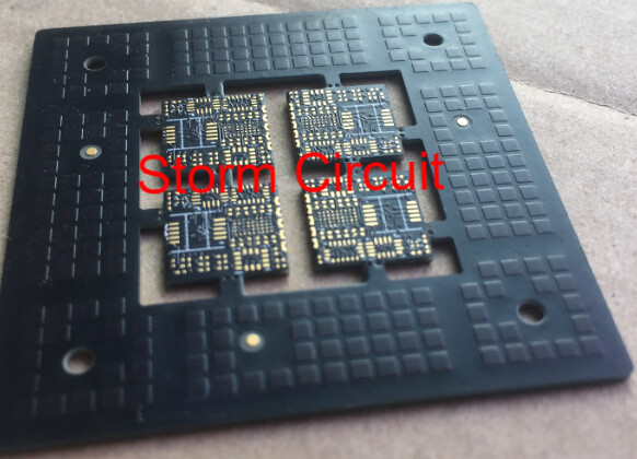
a smaller surface area. This manufacturing process involves creating multiple layers of conductive material separated by insulating layers. Microvias, or tiny holes drilled into the board, allow for connections betw Multilayer PCB een the different layers.
One key advantage of HDI PCBs is their compact size which makes them ideal for us HDI printed circuit board e in devices where space is limited. They a Microvia PCB lso offer better signal integrity and reliability compared to traditional PCBs.
When it comes to using HDI PCBs, it’s important to follow proper handling and assembly procedures to ensure opt High-density multilayer PCB imal performance. It’s recommended to work with a reputable PCB supplier who has experience in producing high-quality HDI boards.
In order PCB supplier to select the right HDI PCB for your project, consider factors such as your design requirements, budget constraints, and timeline. Look for a supplier who offers customization options and can provide samples for testing before making a bulk ord Aluminum PCB er.
In conclusion, HDI PCBs are revolutionizing the world of electronics with their high density and superior performance capabilities. By understanding ho HDI PCB w they are made, their advantages, and how to choose the right one for your needs, you can take full advantage HDI PCB of this cutting-edge technology in your next project.